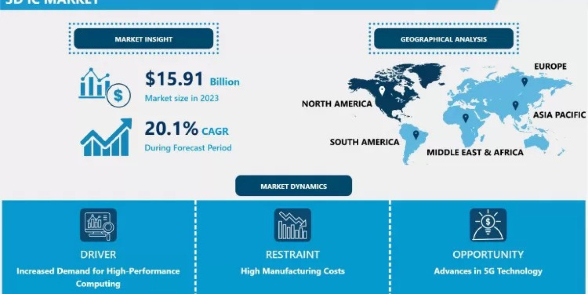
According to a new report published by Introspective Market Research, the Global 3D Integrated Circuit (IC) Market by Product Type, Application, and End-Use Industry, valued at USD 15.91 Billion in 2023, is projected to reach USD 82.73 Billion by 2032, growing at an exceptional CAGR of 20.10% from 2024 to 2032. This explosive growth is driven by the insatiable demand for higher performance and energy efficiency in computing, the end of traditional Moore's Law scaling, and the proliferation of advanced applications like artificial intelligence (AI), high-performance computing (HPC), and 5G/6G connectivity.
3D Integrated Circuits (3D ICs) represent a revolutionary semiconductor packaging and integration technology where multiple silicon dies (chiplets) containing different functionalities (e.g., logic, memory, sensors) are vertically stacked and interconnected using advanced techniques like Through-Silicon Vias (TSVs) and hybrid bonding. This architecture offers transformative advantages over conventional 2D planar chips, including dramatically reduced interconnect lengths, which lead to faster data transfer, lower power consumption, and a significantly smaller footprint. By enabling heterogeneous integration of diverse process nodes and materials (e.g., silicon, compound semiconductors), 3D ICs overcome the limitations of monolithic scaling, allowing for continued performance gains and novel system architectures.
A Key Growth Driver: The Insatiable Demand for AI and High-Performance Computing
A primary force propelling the 3D IC market is the explosive growth of Artificial Intelligence (AI), machine learning, and data-intensive high-performance computing (HPC). These workloads require massive parallelism and constant, high-bandwidth data movement between processors and memory. Traditional 2D architectures create a "memory wall" where data transfer speed limits overall system performance. 3D ICs, particularly those integrating logic processors with 3D-stacked High Bandwidth Memory (HBM), provide a solution by placing memory directly atop or adjacent to the processor using thousands of ultra-fast vertical interconnects. This drastically reduces latency and power consumption while multiplying bandwidth, making 3D ICs an enabling technology for next-generation AI accelerators, supercomputers, and cloud server chips.
A Key Market Opportunity: The Rise of Chiplet-Based Ecosystem and Design Innovation
A monumental market opportunity lies in the establishment of a robust chiplet ecosystem and the resulting design freedom it enables. The chiplet model, where complex systems are built by integrating smaller, pre-validated functional blocks (chiplets) in a 2.5D or 3D package, lowers design costs, improves yield, and accelerates time-to-market. This shift creates opportunities not only for fabless semiconductor companies to mix-and-match best-in-class chiplets from different vendors but also for specialized third-party chiplet designers and advanced packaging foundries. Companies that can provide critical interface standards (e.g., Universal Chiplet Interconnect Express - UCIe), design services, and reliable, high-volume 3D integration platforms will capture significant value in this emerging, disaggregated semiconductor supply chain.
The 3D IC Market is segmented on the basis of Product Type, Application, and End-Use Industry.
Product Type
The Product Type segment is further classified into 3D Stacked Memory, 3D Stacked Logic, 3D Sensor/Image Chips, and Others. Among these, the 3D Stacked Memory sub-segment accounted for the highest market share in 2023. This segment is dominated by High Bandwidth Memory (HBM), which has become the standard for AI and HPC applications. HBM stacks multiple DRAM dies vertically, connected with TSVs, and is typically packaged alongside a GPU or AI processor in a 2.5D arrangement. Its critical role in feeding data to the world's most powerful processors, coupled with its adoption by all major memory and logic vendors, solidifies its leading revenue position in the current market landscape.
Application
The Application segment is further classified into Data Centers & HPC, Consumer Electronics, Automotive, Telecommunications, Medical Devices, and Others. Among these, the Data Centers & High-Performance Computing sub-segment accounted for the highest market share in 2023. This is the primary beachhead for 3D IC technology, where the performance and power benefits directly translate into competitive advantage and lower total cost of ownership. The massive investment in AI infrastructure by cloud service providers (CSPs) and enterprises is the single largest driver, with leading-edge CPUs, GPUs, and AI accelerators for data centers increasingly relying on 3D integration to meet performance targets.
Some of The Leading/Active Market Players Are:
· Taiwan Semiconductor Manufacturing Company (TSMC) (Taiwan)
· Samsung Electronics Co., Ltd. (South Korea)
· Intel Corporation (USA)
· SK Hynix Inc. (South Korea)
· Advanced Micro Devices, Inc. (AMD) (USA)
· Micron Technology, Inc. (USA)
· NVIDIA Corporation (USA)
· ASE Technology Holding Co., Ltd. (Taiwan)
· Amkor Technology, Inc. (USA)
· IBM Corporation (USA)
· Xperi Corporation (USA) - (Invensas, DBI)
· United Microelectronics Corporation (UMC) (Taiwan)
· GlobalFoundries Inc. (USA)
· Teledyne Technologies Incorporated (USA)
· STMicroelectronics N.V. (Switzerland)
and other active players.
Key Industry Developments
News 1: Major Foundry Unveils Next-Generation 3D Fabrication Platform
In November 2024, TSMC unveiled its next-generation "3DFabric" platform, introducing new system-on-wafer (SoW) and chip-on-wafer-on-substrate (CoWoS) advancements. The platform aims to offer greater integration density and design flexibility for AI and HPC chips, reinforcing its leadership in advanced packaging.
This development underscores how leading-edge foundries are competing on 3D integration capabilities as a core service. As transistor scaling slows, superiority in heterogenous integration and packaging is becoming a key differentiator for winning designs from top fabless companies like AMD, NVIDIA, and Apple.
News 2: Strategic Alliance for Chiplet Interconnect Standard
In July 2024, a broad consortium of semiconductor leaders, including Intel, AMD, Samsung, and several key cloud providers, announced the ratification and expansion of the Universal Chiplet Interconnect Express (UCIe) 2.0 standard. The update focuses on higher bandwidth, improved energy efficiency, and support for advanced packaging forms like 3D stacking.
This alliance is critical for the long-term growth of the 3D IC market. A robust, open chiplet interconnect standard reduces design barriers, fosters a multi-vendor supply chain, and accelerates the adoption of chiplet-based 3D designs across the industry, moving beyond proprietary solutions.
Key Findings of the Study
· The 3D Stacked Memory product type and Data Centers & HPC application segment dominate current market revenue.
· The Asia-Pacific region is the largest market, housing major foundries and memory manufacturers, while North America is a leader in design and innovation.
· Key growth is driven by demand for AI/HPC, the need for beyond-Moore's-Law scaling, and the adoption of chiplet architectures.
· Major trends include the standardization of chiplet interfaces (UCIe) and the convergence of packaging and front-end processes.
· The market is led by integrated device manufacturers (IDMs), pure-play foundries, and memory giants, with packaging OSATs playing a crucial role.


